
Internal Plane Information
Contents
Parent page: PCB Dialogs
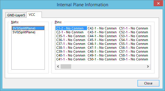
The Internal Plane Information dialog.
Summary
This dialog provides the designer with information about the internal plane layers used in the board design, including the net(s) connecting to them, and the pins (pads) of components associated to those nets.
Access
The dialog is accessed from the PCB Editor, by clicking the Pwr/Gnd button, on the Nets tab of the PCB Information dialog. The latter is accessed by clicking Outputs | Reports | ![]() , from the main menus.
, from the main menus.
Options/Controls
The dialog has no controls in the traditional sense of configuration and management, rather it is simply a presentation of read-only information. Each defined internal plane layer in the layer stackup has its own tab in the dialog, presenting information across the following two regions:
- Nets - a listing of the net(s) associated to the internal plane layer. Multiple nets can be associated to a plane layer through creation of split planes.
- Pins - a listing of the pins (pads) of components associated to the selected net. For each entry in the list, the identifier for the pin is shown (in the format <ComponentDesignator>-<PinDesignator>), as well as information on whether the pin connects to the plane layer, and the type of connection (Direct, Relief), or not (No Connxn).