
Pad
Contents
Parent page: PCB Dialogs
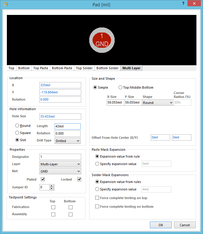
The Pad Dialog.
Summary
This dialog allows the designer to specify the properties of a Pad object. A pad is used to create the electrical connection and mounting point for a component pin. Pads, along with other objects such as lines, are placed in the PCB Library editor to create a footprint for the component to be mounted on. Pads can be single layer or multi-layer (exist on every signal layer). Pads can have a hole, which can be round, square or a slot. The hole is centered by default, but can also be offset if required.
Access
This dialog can be accessed during placement by pressing the Tab key.
After placement, the dialog can be accessed in the following ways:
- Double-click on a placed object.
- Place the cursor over the object, right-click and choose Properties from the context menu.
Options/Controls
Location
- X - The current X position of the center of the pad, relative to the current origin. Edit the value to change the position of the pad relative to the origin.
- Y - The current Y position of the center of the pad, relative to the current origin. Edit the value to change the position of the pad relative to the origin.
- Rotation - The current pad rotation in degrees, edit to change the rotation of the pad. Minimum angular resolution is 0.001°.
Hole Information
- Hole Size - The current hole size for the pad. The value specifies the diameter of the hole (in mils or mm) to be drilled in the pad during fabrication. For a single-layer pad (such as an SMD pad or edge connector), this is automatically set to zero. The hole size can be set from 0 to 1000mil, and can be set larger than the pad area to define copper free mechanical holes. Edit the value in this field to change the pad hole size. Values can be entered in either mm or mil units.
Choose one of the following options to specify the shape of the hole:
- Round - specifies a round hole shape (default) for the pad. With this shape option enabled, the Drill Type field will become available.
- Square - specifies a square (punched) hole shape for the pad. With this shape option enabled, the Rotation field will become available.
- Slot - specifies a round ended slotted hole shape for the pad. With this shape option enabled, Length, Rotation and Drill Type fields will become available.
As mentioned above, one or more of the following additional fields become available, dependent on the shape type chosen:
- Length - applicable for slotted holes only, this is the end-to-end slot length for the hole in the pad. The value specifies the length of the slot in mm or mil, to be NC routed in the pad during fabrication. The hole size can be set from 0 to 1000mil. The Length must be larger that the Hole Size to define a valid slot, and can be set larger than the pad to define (copper free) mechanical slot holes.
- Rotation - applicable to square and slotted holes, this is the rotation of the hole, in degrees. Minimum angular resolution is 0.001°.
- Drill Type - applicable to round and slotted holes, use this field to specify how the hole is to be created. Choose from Drilled, Punched, Laser Drilled, or Plasma Drilled.
Properties
- Designator - The current pad designator. If the pad is part of a component, the designator is usually set to the corresponding component pin number. The designator can be up to 20 characters in length and cannot include any spaces. Free pads can include a designator, or the field can be left empty. If the designator begins or ends with a number, the number will auto-increment when placing a series of pads sequentially. Edit the value in this field to change the pad designator. Note that multiple pads within the same component footprint can share the same designator, if required.
- Layer - The layer the pad is currently assigned to. Pads can be assigned to any available layer, Set the Layer to
Multi-Layerto define a pad shape on all signal layers. - Net - The net that the pad is currently assigned to. Change the net assignment by clicking in the field and choosing a net from the drop down list. Select No Net to specify that the pad is not connected to any net. The Net property of a primitive is used by the Design Rule Checker to determine if a PCB object is legally placed.
- Plated - This option determines whether or not the pad has a plated hole. If both plated and non-plated pads exist in a design, the non-plated holes will be set to use different tools from the plated holes in the NC drill files.
- Locked - Enable to protect the pad from being edited graphically. Lock a pad whose position or size is critical. If you try to edit a primitive that is locked, you will be informed that the primitive is locked and asked if you wish to proceed with the action. If this option is unchecked, the primitive can be freely edited without confirmation. Note that the Locked checkbox has no effect on a pad that belongs to a component, if the component is not locked the pads will move when the component is moved. In this situation, lock the component to prevent accidental movement.
- Jumper ID - Set the Jumper ID to a non-zero value (range of 1-1000) to indicate that this pad is part of a jumper component footprint. Jumper components can be used on a single-sided PCB when there will be a wire link that physically connects the pads together, rather than using tracks to create the connection. The Jumper ID value tells the software which pads to treat as 'connected'. A jumper connection can only be created between the pads within the same component footprint, they must have the same Jumper ID value, and must also be assigned the same net. The component must also have its Type set to Jumper. When these conditions are met, a jumper connection is shown as a curved connection line in the PCB Editor.
Testpoint Settings
Use the Testpoint Settings to define this pad as a testpoint for Fabrication and/or Assembly testpoint file generation. A testpoint is a location where a test probe can make contact with the PCB to check for correct function of the board. Any pad or via can be nominated as a testpoint, when this is done the component that the pad or via belongs to, automatically gets locked.
- Top - Enable this option for this pad to be defined as a top layer testpoint.
- Bottom - Enable this option for this pad to be defined as a bottom layer testpoint.
Size and Shape
The copper area (land area) of the pad is defined by the X and Y size, and the Shape setting.
- Simple - A simple pad is one whose size and shape is identical on all layers.
- Top-Middle-Bottom - A Top-Middle-Bottom layered pad supports defining different X & Y sizes and shape for the Top layer, for all mid signal layers, and for the Bottom layer, separately.
- X-Size - The current X (horizontal) size of the pad, enter a value from 1 to 10000mil. The X and Y size can be set independently to define asymmetric pad shapes.
- Y-Size - The current Y (vertical) size of the pad, enter a value from 1 to 10000mil. The X and Y size can be set independently to define asymmetric pad shapes.
- Shape - The basic pad shape. Basic pad shapes include
Round,Rectangular,Octagonal, orRounded Rectangle. The basic shape can be manipulated by changing the X and Y size settings to produce an asymmetrical pad shape. - Corner Radius - Available when the Shape is set to
Rounded Rectangle. The value is a percentage of half of the shortest side of the pad. As such, a value of 0% corresponds to a rectangular pad, and 100% to a circular pad. - Offset From Hole Center (X/Y) - Enter a value to offset the pad land area from the center of the pad hole, by this amount.
Paste Mask Expansion
An opening in the paste mask is automatically created by the software, the same shape as the pad. This opening can be larger (a positive expansion value) or smaller (a negative expansion value) than the pad itself, as defined by the Paste Mask Expansion setting. Typically paste mask openings are smaller than the pad, but there are exceptions to this.
- Expansion value from rules - When this option is enabled the paste mask expansion for this pad is defined by the applicable Paste Mask Expansion design rule.
- Specify expansion value - Enable this option to override the rule and specify the paste mask expansion value for this pad.
Solder Mask Expansions
An opening in the solder mask is automatically created by the software, the same shape as the pad. This opening can be larger (a positive expansion value) or smaller (a negative expansion value) than the pad itself, as defined by the Solder Mask Expansion setting. Typically solder mask openings are larger than the pad, but there are exceptions to this.
- Expansion value from rules - When this option is enabled the solder mask expansion for this pad is defined by the applicable Solder Mask Expansion design rule.
- Specify expansion value - Enable this option to override the rule and specify the solder mask expansion value for this pad.
- Force complete tenting on top - The term tenting means to close off. If this option is enabled then the settings in the applicable solder mask expansion design rule will be overridden, resulting in no opening in the solder mask on the top solder mask layer for this pad. When this option is enabled, the Expansion value from rules and the Specify expansion value options are ignored.
- Force complete tenting on bottom - The term tenting means to close off. If this option is enabled then the settings in the applicable solder mask expansion design rule will be overridden, resulting in no opening in the solder mask on the bottom solder mask layer for this pad. When this option is enabled, the Expansion value from rules and the Specify expansion value options are ignored.