Pin
Contents
Parent page: Schematic Objects
The schematic Pin represents the physical component pin in the schematic design space.
Summary
A pin is an electrical design primitive. Pins give a component (part) its electrical properties and define the connection points on the part for the incoming and outgoing signals.
Availability
Pins can only be placed in the Schematic Library Editor. Use one of the following methods to place a pin:
- Click Home | Place |
 from the main menus.
- Click the Add button in the Pin List region of the SCH Library panel.
- Click the Add button in the Component Pin Editor dialog (accessed by clicking the Edit Pins button in the Library Component Properties dialog).
Placement
New pins are added to the component that is currently visible in the Schematic Library Editor, select the required component in the SCH Library panel.
- Using one of the first two techniques described above, invoke the pin placement process. Note that the floating pin is held by the electrical end, which must be positioned away from the component body. Only one end of the pin is electrical, and it is always this end the pin is held by.
- Since there is often numerous pins on a component, it is more efficient to edit the properties of each pin as they are being placed. To do this, press Tab while the pin is floating on the cursor.
- Edit the pin properties as required, typically this will include at least the Display Name, Designator and Electrical Type (refer to the image of the Pin Properties dialog further down the page). Note that you can move between these fields using the Tab key to step forward, or Shift+Tab keys to step backward. You can also accept the dialog settings by pressing the Enter key on the keyboard, making it possible to define the dialog settings without touching the mouse.
- Press the Spacebar to rotate the pin if required. Rotation is anti-clockwise in steps of 90 degrees.
- Position the pin, then click or press Enter to place the pin in the Library Editor workspace.
- Continue to place pins, or right-click or press Esc to terminate pin placement.
Adding Pins in the Component Pin Editor
Pins can also be added through the Component Pin Editor dialog, which is accessed via the Edit Pins button in the Library Component Properties dialog.
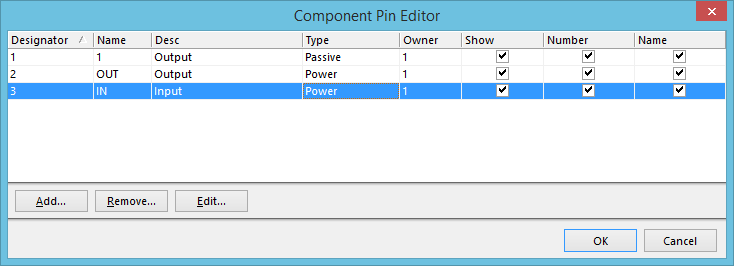
Add one or more pins in the Component Pin Editor dialog.
Click the Add button to add a new pin, then define the properties in the Component Pin Editor dialog. Note that multiple pins can be added and their properties defined - you can also use Tab and Shift+Tab to step between the fields. When you click OK to close the dialog, the new pin(s) are placed on the sheet to the bottom right of the component, ready to be positioned.
Notes on Pin Numbering
For many components there will be a series of pins that have numerical names and numbers. The auto-increment feature can be used to speed the placement of these pins. Auto-increment is invoked automatically if the pin properties are edited before placement (press Tab while the pin is floating on the cursor). The feature works for both the Designator and the Display Name - the pin Designator uses the Primary auto-increment field and the pin Display Name uses the Secondary auto-increment field. It supports incrementing alpha and numeric values, and decrementing numeric values.
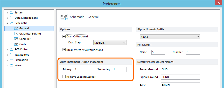 Configure the Auto-increment settings on the Schematic - General page of the Preferences dialog.
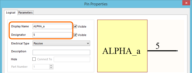 Enter the Display Name and Designator pin properties.
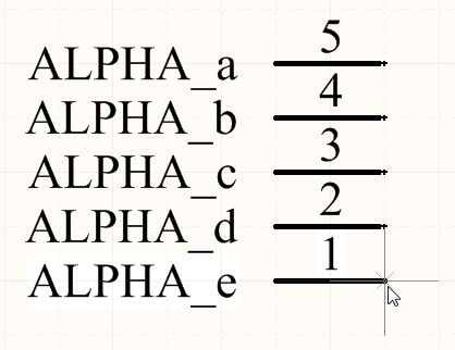 Note the incrementing alpha pin name and decrementing numeric pin number.
Use the auto-increment feature to speed the placement of pins.
Graphical Editing
To move a pin, click and hold on it - the cursor will jump to the electrical hotspot end of the pin - then move it to the new location, placing it with the electrical end away from the component body.
While dragging, the pin can be rotated (Spacebar/Shift+Spacebar) or mirrored (X or Y keys to mirror along the X-axis or Y-axis respectively).
Non-Graphical Editing
The following methods of non-graphical editing are available:
Via an Associated Properties Dialog
Dialog page: Pin Properties
This method of editing uses the Pin Properties dialog to modify the properties of a pin object.
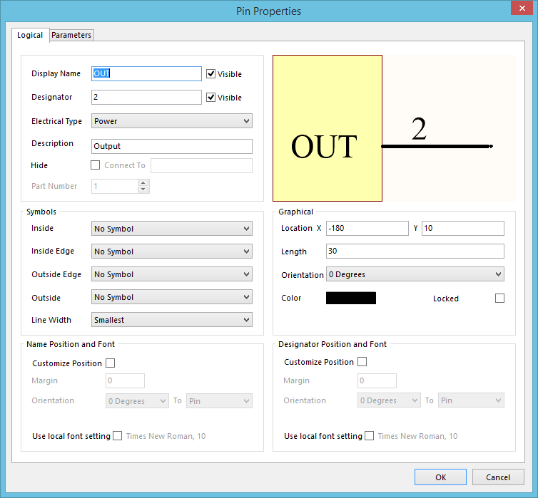
The Pin Properties dialog.
The dialog can be accessed during placement by pressing the Tab key.
After placement, the dialog can be accessed in one of the following ways:
- Double-clicking on the placed pin object.
- Placing the cursor over the pin object, right-clicking and choosing Properties from the context menu.
Pin Display Name & Designator - Position & Font
The location of the pin Display Name and pin Designator (number) is defined globally by the Pin Margin settings on the Schematic - General page of the Preferences dialog. This is an environment setting, meaning it applies for the PC where the setting is defined. The settings define a relative distance the text is away from the non-electrical end of the pin.
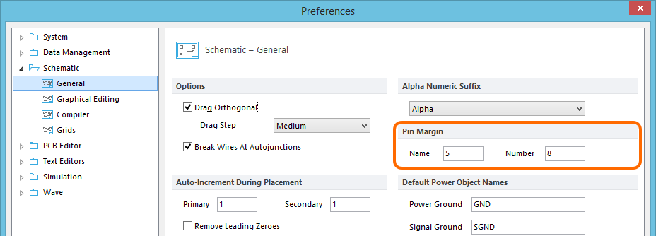
Set the distance of the pin text (Pin Margin) in the Preferences dialog.
The font used for the pin Display Name and pin Designator (number) - for a component placed on a schematic sheet - is defined at the document level in the Document Options dialog - click the Change System Font button to set it.
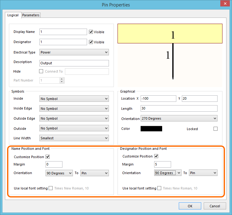
For pins, these system-level settings of position and font can be overridden locally. Controls for customization of the position and font for a pin's Name and Designator can be found on the Logical tab of the Pin Properties dialog, when editing a pin in either the Schematic Library or Schematic Editors. While the controls themselves are the same for both attributes, separate sets of controls allow them to be customized independently of each other.
The font and location of the pin Display Name and pin Designator (number) can be modified for individual pins, if required.
Use the Customize Position option to change from following the default settings for position, to an overriding, customized position. For the Margin, simply enter a new value directly in the associated field. For the Orientation, use the drop downs to choose the angle (0 Degrees or 90 Degrees) and the reference (Pin or Component).
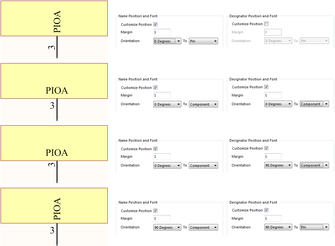
Example customized positions for pin Display Name and Designator.
Use the Use local font setting option to change from following the default system font, to an overriding, customized font. To do so, simply click on the font control to the right of the option to access the standard Font dialog. The control doubles as a notification for the font currently chosen, or 'in-force'.

Example customization of the font for a pin's Display Name.
Pin Symbol Line Width
When representing a component in the schematic editing domain, each pin defined as part of that device's schematic symbol can have one or more symbols displayed. These are symbols displayed on the Inside, Inside Edge, Outside, or Outside Edge, in relation to the main component symbol outline, as required. Examples might include a Clock symbol on the Inside Edge, or a Dot symbol on the Outside Edge. Such symbols greatly improve the readability of the design, through visual indication of the purpose of the signal traversing a particular pin.
Use the Line Width property - available in the Symbols region of the Pin Properties dialog - to determine the width of the line used to draw these symbols. Choose from either Small or Smallest.
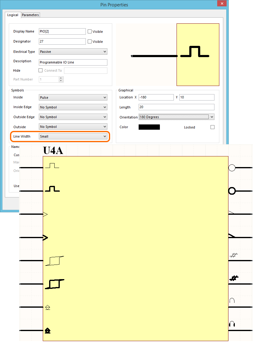
Example pin symbols displayed using the two supported settings for Line Width.
Via the SCHLIB Inspector Panel
Panel page: SCHLIB Inspector
The SCHLIB Inspector panel enables the designer to interrogate and edit the properties of one or more design objects in the active document. Used in conjunction with the Find Similar Objects dialog, the panel can be used to make changes to multiple objects of the same kind, from one convenient location.