PCB
Contents
Parent page: PCB Panels

The PCB panel gives you full access to board objects and items via a filtered browser.
Summary
The PCB panel allows you to browse the current PCB design using a range of filter modes to determine which object types or design elements are listed, highlighted or selected. The panel also has editing modes for specific object types or design elements that provide dedicated controls for editing procedures. Note that you can access the properties for any element listed in the panel.
Panel Access
To open the PCB panel click the View | PCB | ![]() button, or use its secondary button
button, or use its secondary button ![]() and the associated drop-down menu to open the PCB panel in a particular browsing mode.
and the associated drop-down menu to open the PCB panel in a particular browsing mode.
Panels can be configured to be floating in the editor space or docked to sides of the screen. If the PCB panel is currently in the group of docked Workspace panels on the left, use the PCB tab located at the bottom of the panels to bring it to the front.
If already open and docked in the Workspace panels, use the PCB tab to access the PCB panel.
Panel browsing modes
The top drop-down list in the panel is where you select the panel mode. The mode can be set to browse nets, components, polygons, or set to use the Split-Plane, Differential Pairs or Hole Size Editors.
Select the browsing mode using the top pull-down list.
In any of the modes, as you click on an entry in a subsequent region of the panel a filter is applied, essentially using the entry as its scope.
Setting the visual filtering
The visual result of the applied filtering on the document in the design editor window is determined by a series of highlighting controls toward the top of the panel. The effect that is imposed in the editor view can be set to Normal, Mask or Dim, where in practice, Mask has the most obvious highlighting effect.
The Normal / Mask / Dim dropdown list provides options for visibly contrasting filtered and unfiltered objects within the design editor window.
Select the type of visual filtering applied using the masking mode drop-down list.
The visual highlighting effect for each masking mode:
- Normal - Filtered objects are visible in the design editor window and the appearance of unfiltered objects remains unchanged.
- Mask - Filtered objects are highlighted in the design editor window, with all other objects made monochrome
- Dim - Filtered objects are highlighted in the design editor window, with all other objects retaining their colors, but shaded.
Display control
In Mask view mode, unfiltered (not selected) objects are monochrome. To set the contrast of the background (un-highlighted) objects, use the Mask Level slider control available in the Highlight & Edit Mask group under the View tab.
Similarly, in Dim view mode unfiltered objects retain their colors, but are shaded. Set the balance between filtered and unfiltered objects using the Dim Level slider available in the Highlight & Edit Mask group under the View tab, as shown above.
Use the ![]() button to remove the display highlighting.
button to remove the display highlighting.
Filter options
The panel's three checkboxes apply these filter actions:
- Select - when enabled, the filtered objects will be selected in the workspace.
- Zoom - when enabled (default), the filtered objects will be zoomed and centered (where possible) in the design editor window. Use the button to adjust the zoom factor that will be used to close-in on filtered objects.
- Clear Existing - when enabled (default), any existing filter will be cleared before applying a new one. Disabling this option allows you to extend an existing filter, essentially refining the filter further by applying a new filter in addition to the existing one.
Any combination of these options can be enabled. For example, you might want to have all filtered objects zoomed, centered and selected in the design editor window, whilst applying masking to take away the clutter of other design objects.
Use the ![]() button to disable the currently-applied filter. All objects in the design workspace will become fully visible and available for selection/editing. If you wish to re-apply the filter, click the
button to disable the currently-applied filter. All objects in the design workspace will become fully visible and available for selection/editing. If you wish to re-apply the filter, click the ![]() button.
button.
Panel mini-viewer
The bottom section of the PCB panel provides a mini-viewer for the current document, with an image of the current board design central to its window. A white viewing box is imposed on the image to show the area currently displayed in the design editor window. As the editor display automatically pans and zooms in response to the PCB panel filter selections, the box moves and expands accordingly to indicate the board viewing area.
The mini-viewer automatically window pans and zooms to reflect the status of the main editor window.
As you manually pan around the document in the design editor window – using the editor's horizontal and vertical scrollbars or the right-click panning hand – the viewing box in the panel will also move accordingly. Conversely, moving the viewing box around inside the mini-viewer (using click and drag) will cause the document in the design editor window to pan accordingly, at the current zoom level.
As you zoom in or out in the design editor window, the viewing box will be resized accordingly in the panel mini-viewer. Conversely, resizing the viewing box in the mini-viewer – by clicking and dragging any of its vertices – will cause the document zoom level to change in the design editor window. The smaller the size of the viewing box, the greater the zoom level for the actual document.
Browsing Nets
Select Nets from the PCB panel's drop-down list. The two main list regions of the panel will change to reflect an object hierarchy, in order from the top:
- Nets defined in the board design.
- Individual primitive items within a Net (pads, vias, tracks and fills).
The PCB panel regions allow a cumulative filter selection through individual nets to net items (primitives).
Right-clicking on a Net or net Primitive item entry and choosing the Properties command from the associated context menu (or double-clicking on the entry directly) will provide access to the relevant Properties dialog, from where you can view or modify the properties of the selected net or item.
The display/inclusion of each net item type, in the Net Items region of the panel, is dependent on whether the corresponding option for each has been enabled on the right-click menu, accessed from either the Nets or Net Items regions.
Right-click on a net or net item entry to select the included items.
In practice, as you click on an entry in the panel's list, a filter will be applied based on that entry. The visual result of the selection (in the design editor window) is determined by the highlighting methods enabled (Mask/Dim/Normal, Select, Zoom). Multiple entries can be selected in each region, using standard Shift+click and Ctrl+click methods.
Multiple nets selected, with the visual mode set to Mask.
Browsing Components
Place the panel in Components mode by selecting Components from the drop-down list at the top of the panel. The two main list regions of the panel will change to reflect an object hierarchy, in order from the top:
- Components on the board.
- Individual primitives that constitute a Component (pads, tracks and arcs).
The PCB panel regions allow a cumulative filter selection through individual components to component primitives.
Right-clicking on a component or component primitive entry and choosing the Properties command from the associated context menu (or double-clicking on the entry directly) will provide access to the relevant Properties dialog, from where you can view/modify the properties of the component/primitive as required.
The display/inclusion of each component primitive type, in the Component Primitives region of the panel, is dependent on whether the corresponding option for each has been enabled on the right-click menu, accessed from either the Components or Component Primitives regions.
Right-click on a component or component primitive entry to select what items are included.
In summary, as you click on an entry in the panel's list, a filter will be applied based on that entry. The visual result of the selection (in the design editor window) is determined by the highlighting methods enabled (Mask/Dim/Normal, Select, Zoom). Multiple entries can be selected in each region, using standard Shift+click and Ctrl+click methods.
Three components selected, with the visual mode set to Mask.
Using the Split Plane Editor
Place the panel in Split Plane Editor mode by selecting Split Plane Editor from the drop-down list at the top of the panel.
The Nets/Layers section of the panel will fill with all internal plane layers currently defined for the design. Within that section, the Split Count column indicates how many split planes exist for the corresponding plane layer. A split count of 1 effectively means that the layer has not been split, and the layer itself is considered to be a single split.
As you select an entry in the Layers section, all of the split planes on that plane layer and their assigned nets will be loaded into the Split Planes area of the panel. To view only nets associated with split planes in this section, ensure that the Show Split Plane Nets Only option is enabled on the right-click menu. For each entry, a Node Count is displayed. This value reflects the total number of pads and vias that are connected to that split plane region.
Filtering will be applied based on the entry chosen in the Layers section, the visual result of which (in the design editor window) is determined by the highlighting methods enabled (Mask/Dim/Normal, Select, Zoom). Multiple entries can be selected using standard Shift+click and Ctrl+click methods.
As you select an entry in the Split Planes section of the panel, filtering will be applied based on that entry. Again, the filtering results depend on the highlighting methods enabled and whether pads and/or vias are enabled with respect to their visibility. Multiple entries can be selected in the region.
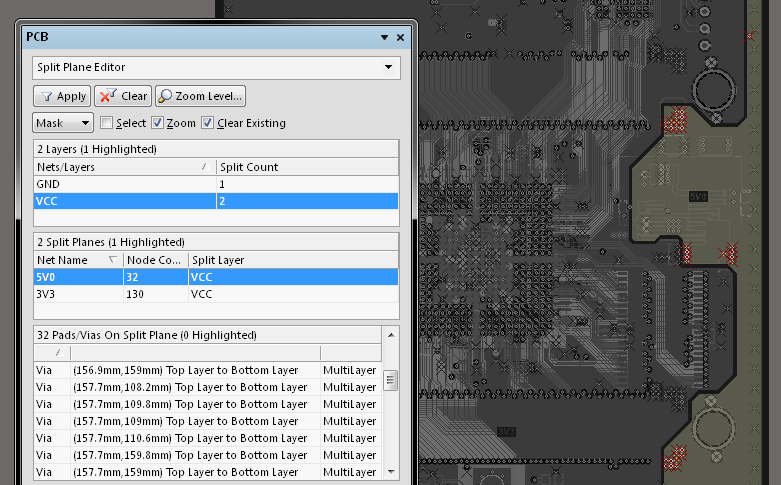
Here, the VCC layer has a 3V3 and 5V0 region split. The selected 5V0 split is visible as the highlighted region (and vias) on the right. Viewed in Single Layer Mode.
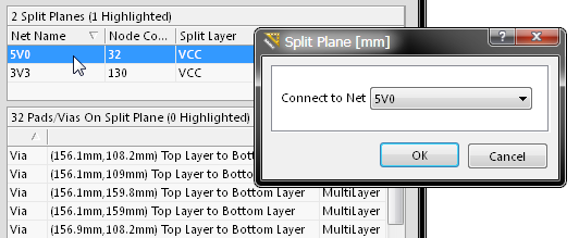
Double-click on an entry (or select Properties from the right-click menu) to bring up the Split Plane dialog, from where you can change the net to which the split plane region is connected. Choose from any of the currently loaded nets for the design.
The Pads/Vias On Split Plane section of the panel lists each of the pads and/or vias connecting to the split plane region selected in the Split Planes section. Entries will only appear if the corresponding Show Pads and/or Show Vias options have been enabled from the right-click menu.
As a pad or via entry is selected, filtering will be applied based on that entry. With masking applied, the selected pad/via entry will be highlighted in the editor workspace. If you wish to see where a pad or via resides in relation to the split plane region, click on that region within the design workspace before clicking a pad/via entry. Again, multiple entries can be chosen from the list.
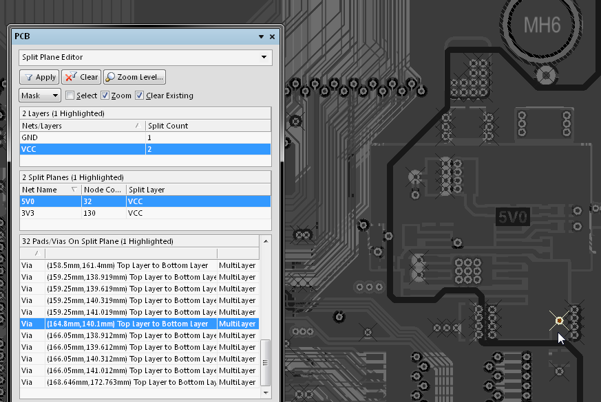
A selected Via can be seen highlighted in the board's 5V0 split plane region (shown near the mouse arrow). The VCC Layer has been selected as the editor view.
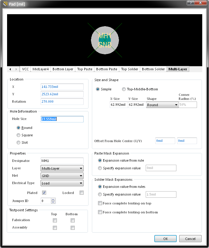
In the panel's Pads/Vias On Split Plane section, right-clicking on a pad or via entry and choosing the Properties command will open the relevant properties dialog, from where you can view/modify the properties of the pad/via as required.
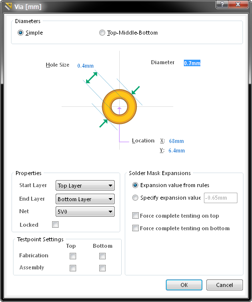
Right-click a Via/Pad in the list and select Properties to open the Via/Pad Properties dialog.
Browsing Polygons
Place the panel in Polygons mode by selecting Polygons from the drop-down list at the top of the panel. The two main list regions of the panel will change to reflect, in order from the top:
- Polygons within the board design.
- Individual primitives that constitute a Polygon (tracks, arcs and regions).
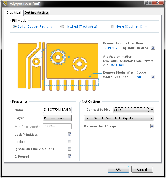
In the PCB panel, right-clicking on a polygon entry and selecting Properties (or double-clicking on the entry directly) will open the Polygon Pour dialog, from where the Polygon properties can be viewed or modified as required.
Similarly, right-clicking on a polygon primitive entry and selecting Properties (or double-clicking on the entry directly) will provide access to the relevant properties dialog, such as the Regions dialog, from where the properties of the primitive can be viewed and modified as required.
In the PCB panel's Polygon Primitives region, the display/inclusion of each polygon primitive type is dependent on the setting of corresponding enabling option, accessed from right-click menu.
As a Polygon Primitive entry is selected in the PCB panel's list a filter will be applied based on that entry, where the visual result of which (in the design editor window) is determined by the enabled highlighting methods (Mask/Dim/Normal, Select, Zoom). Multiple entries can be selected in each region, using standard Shift+click and Ctrl+click methods.
Polygons are formed by multiple primitives such as tracks, arcs and regions. Two regions are selected above, and the PCB view set to Dim.
Using the Hole Size Editor
Place the PCB panel in Hole Size Editor mode by selecting Hole Size Editor from the drop-down list at the top of the panel. The three main list regions of the panel will change to reflect, in order from the top:
- The general filtering for hole types and their status.
- Hole objects arranged in groups, as determined by size and shape.
- Individual primitives that constitute each group of hole objects (pads, vias and slots).
The three panel sections show the cumulative filtering applied to hole types, styles and status.
The groups of holes can be collectively edited in the Unique Holes section of the panel by entering values in the appropriate column cell. You can enter a value in mm to change the current hole size for pads and vias in the Hole Size column.
Editing the hole size for the selected group of six matching hole styles.
You can also change the corresponding Length, Type, Plated and Symbol entries for holes where applicable.
Changing the hole type (from round to square) for the selected group of six matching hole styles.
Individual pad/via objects belonging to the selected holes group are listed in the lower Pad/Via section of the PCB panel. Right-clicking on an object in the list and selecting Properties (or double-clicking on the entry directly) will open the matching dialog for that primitive, where its properties can be viewed and edited.
As you click on an entry in the PCB panel's lists a cumulative filter will be applied based on that entry. The visual result of this (in the design editor window) is determined by the highlighting methods enabled (Mask/Dim/Normal, Select, Zoom). In this way you can quickly highlight all holes of a particular status, holes of a particular style or size, or an individual hole primitive (pad/via) that exits in that filtered group. Multiple entries can be selected in each list section, using standard Shift+click and Ctrl+click methods.

The panel selections filter down to hole primitives of a specific type. Four are selected and displayed here from the '0.75mm & Round' group, as selected above.
Browsing 3D Models
Place the PCB panel in 3D Models mode by selecting 3D Models from the drop-down list at the top of the panel. Change to 3D viewing mode through the Switch to 3D button ![]() under the View tab, or use the '3' shortcut.
under the View tab, or use the '3' shortcut.
The two main list regions of the panel when in 3D Model mode reflect, in order from the top:
- Specific components that have associated 3D body object(s) or free models (non-PCB mounted, free-floating 3D bodies).
- The individual 3D bodies for each component or free model.
The PCB panel's filter scope progresses through components to their constituent model elements, while the visual result tracks the changes.
As you select a specific component in the Components region of the panel, filtering will be applied using the component as the scope of the filter. The visual result (in the design editor window) is determined by the highlighting methods enabled (Mask/Dim/Normal, Select, Zoom). Multiple rule entries can be selected using standard Shift+Click and Ctrl+Click features.
Double-clicking a component entry in the Component region of the panel (or right-clicking and choosing Properties) will open the relevant Component dialog, from where you can edit its properties in detail.
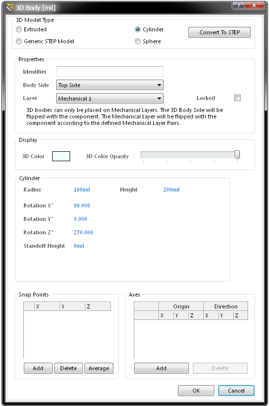
Similarly, double-clicking a model entry in the Models region of the panel (or right-clicking and choosing Properties) will open the relevant 3D Body dialog, from where you can edit the complete 3D body properties. Note that the Type can be Extruded, Cylinder, Sphere or a Generic STEP model.
When selecting a component's constituent models from the Models list area in the PCB panel, the view in the editor workspace will zoom, dim/mask or select accordingly.
An individual model selected from a component. In this case, a cylinder from the component LED2.
The PCB panel can be used to select display properties for 3D models. The cone icons ![]() represent different levels of transparency from 100% (hidden) down to 0% (solid) in increments of 25%. You can select multiple components and apply the same display controls to them at once using the Highlighted Models options.
represent different levels of transparency from 100% (hidden) down to 0% (solid) in increments of 25%. You can select multiple components and apply the same display controls to them at once using the Highlighted Models options.
The selected cylinder model being set to 75% opacity. Multiple models can also be selected and changed in one action.
The 3D Bodies Display Options controls allow you to control the display of 3D bodies, without having to modify the current view configuration. Display options set from the PCB panel are not saved as part of the view configuration.
Multiple Model entries can be selected using standard Shift+Click and Ctrl+Click features, providing full control over the 3D Model view and the base 3D elements that make up a component.
Here, both a cylinder (set to 75% opacity) and a sphere (solid / 0% opacity) from a LED component are selected.
Right-Click Menus
The following is a summary of all right-click menu commands that can appear for the panel. The actual content of the menu varies, depending on the current mode of the panel and the particular region of the panel from where the menu is accessed:
- Select All - quickly select all entries in the section of the panel from which the right-click menu was accessed
- Clear Filter - clear the currently-applied filter. All objects in the design workspace will become fully visible and available for selection/editing
- Report - generate a report in context with the section of the panel the menu is accessed from. After launching the command, the Report Preview dialog will appear from where you can peruse, print and export the report in various file formats
- Properties - access the corresponding properties dialog for the chosen object, from where you can view/modify the properties for that object. For example, with a component entry selected, using this command will access the associated Component dialog.
- Show Pads - enable to display pad entries in the relevant list section of the panel. For example, to display pad entries in the Component Primitives section when in Components mode, or in the Pads/Vias On Split Plane section, when in Split Plane Editor mode
- Show Vias - enable to display via entries in the relevant list section of the panel. For example, to display via entries in the Net Items section when in Nets mode, or in the Pads/Vias On Split Plane section, when in Split Plane Editor mode
- Show Tracks - enable to display track entries in the relevant list section of the panel. For example, to display track entries in the Net Items section when in Nets mode
- Show Arcs - enable to display arc entries in the relevant list section of the panel. For example, to display arc entries in the Component Primitives section when in Components mode
- Show Fills - enable to display fill entries in the relevant list section of the panel. For example, to display fill entries in the Net Items section when in Nets mode
- Show Regions - enable to display region entries in the relevant list section of the panel. For example, to display region entries in the Net Items section when in Nets mode
- Show Component Bodies - enable to display component body entries in the relevant list section of the panel. For example, to display body entries in the Component Primitives section when in Components mode
- Show Strings - enable to display string entries in the relevant list section of the panel. For example, to display string entries in the Net Items section when in Nets mode
- Show Split Plane Nets Only - enable to display only nets connecting to split plane regions, in the Split Planes And Nets section of the panel, when in Split Plane Editor mode
Notes
- Ctrl+click over a selected entry to deselect it. If the entry is the only one selected for that region, performing this action will clear the filter.
- In sections of the panel where multiple columns of data exist, the data may be sorted by any column by clicking on the header for that column. Clicking once will sort in ascending order. Click again to sort by descending order.
- You can change the order in which columns of data are displayed. To move a column, click on its header and drag it horizontally to the required position. A valid position is indicated by the appearance of two green positional arrows.