Project Options - Connection Matrix
Parent page: WorkspaceManager Dialogs
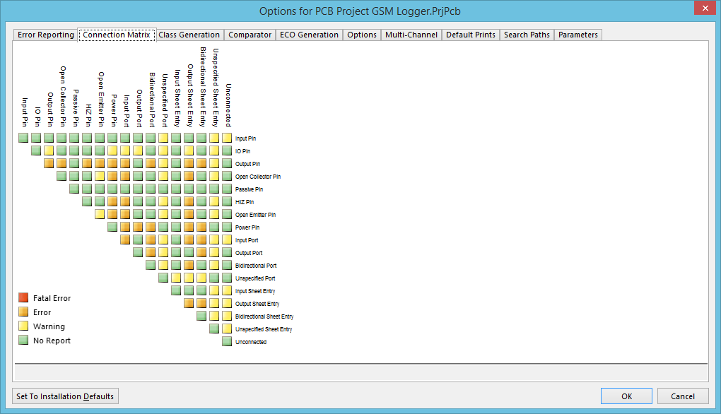
The Connection Matrix tab of the Options for PCB Project dialog.
Summary
This tab of the Options for PCB Project dialog delivers a matrix providing a mechanism to establish connectivity rules between component pins and net identifiers, such as Ports and Sheet Entries. It defines the logical or electrical conditions that are to be reported as warnings or errors. For example, an output pin connected to another output pin would normally be regarded as an error condition, but two connected passive pins would not.
When the project is compiled, these violation settings will be used - in conjunction with the defined settings on the Error Reporting tab - to test the source documents for violations. Any violations that are found and have a report level of Warning, Error or Fatal Error, will be displayed as violation messages in the Messages panel. In addition, if compiler errors and warnings are enabled for display on the schematic (enabled on the Schematic - Compiler page of the Preferences dialog), an offending object will display a colored squiggle beneath it.
Access
This is one of multiple tabs available when configuring the options for a project – accessed from within the Options for Project dialog. This dialog is accessed by:
- Clicking Project | Content |
 , from the main menus in the Schematic Editor, or the PCB Editor.
 - Right-clicking on the entry for the project itself, on the Projects panel, and choosing Project Options from the context menu.
Options/Controls
Connection Matrix
The matrix presents all possible wiring connection checks, between combinations of pins, ports, and sheet entries, as well as testing for unconnected entities. The matrix is read in an across/down fashion and the color of the matrix element at the row-column intersection specifies how the Compiler will respond when testing for that particular condition.
To change the reporting mode for a violation check in the matrix, simply click on the colored square where the row and column of two entities intersect. Each time you click, the mode will move to the next report level. The following levels are supported:
Right-Click Menu
The following commands are available from the right-click context menu for the tab:
- All Off - set all entries in the matrix to No Report.
- All Warning - set all entries in the matrix to Warning.
- All Error - set all entries in the matrix to Error.
- All Fatal - set all entries in the matrix to Fatal.
- Default - set all entries in the matrix back to their default settings.
Additional Options
- Set To Installation Defaults - click this button to return all entries in the matrix back to their default settings.
Notes
- Use the Error Reporting tab of the Options for PCB Project dialog to specify reporting levels associated with further electrical and drafting violations.
- There may be points in the design which you know will be flagged as electrical violations, which you do not want to be flagged. To suppress these, place a No ERC schematic design directive object at each point.