Properties for Schematic Component
Contents
Parent page: Sch Dialogs
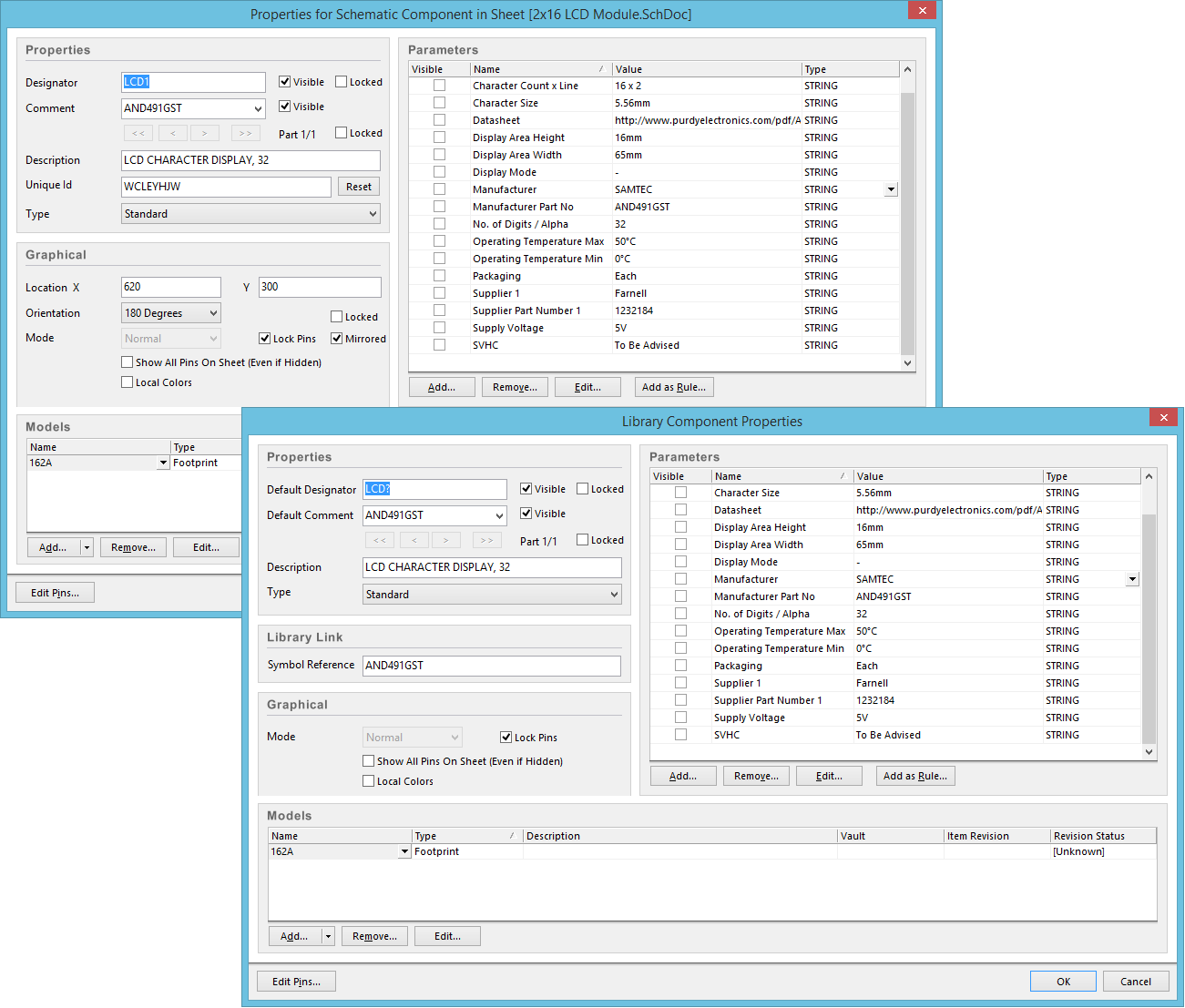
The two incarnations of the Component Properties dialog. At the top, the dialog as it appears for a component
placed/being placed on the schematic. At the bottom, the dialog as it appears for the component in the source
schematic library.
Summary
This dialog allows the designer to edit the properties of a schematic component. The controls of the dialog, and its banner text, will vary depending on the context in which it is accessed. In the Schematic Editor, the dialog (Properties for Schematic Component dialog) is the main properties dialog for a component placed/being placed on a source sheet, while in the Schematic Library Editor, it is the main properties dialog (Library Component Properties dialog) for the symbol being created.
Access
The dialog can be accessed and used in both the Schematic Editor and the Schematic Library Editor.
- Schematic Editor - the dialog can be accessed in the following ways:
- Pressing the Tab key during part placement.
- Double-clicking on the placed part object.
- Placing the cursor over the placed part object, right-clicking and choosing Properties from the context menu.
- Schematic Library Editor - the dialog can be accessed in the following ways:
- Double-clicking on the entry for the component, in the Components region of the SCH Library panel.
- Selecting the required component in the Components region of the SCH Library panel, then clicking the Edit button at the bottom of the region.
- For the active component, selected in the SCH Library panel, using the Home | Library |
 » Component Properties command, from the main menus.
Options/Controls
Properties
- Designator - this field shows the part's logical designator, which identifies the part within the design. If you do not enter a designator before you place a part then its designator will be the pre-assigned default (such as U?, C?, D?, R?).
- Visible - use this option to control the visibility of the designator in the workspace. Enable to display the designator, disable to hide it.
- Locked - enable this option to lock the designator for the part, preventing it from being changed as part of an annotation process.
- Comment - use this field to give the component a meaningful comment, which might be its part number (for a specific IC package), or a value (for a generic component such as a resistor, capacitor, or inductor).
- Visible - use this option to control the visibility of the comment in the workspace. Enable to display the comment, disable to hide it.
- Part - this field indicates which part this particular instance is. For a single part component, the entry will simply be Part 1/1, and all buttons will be unavailable. For a multi-part component, this field will reflect the specific part in the form Part x/y (which part it is (x) out of the total number of defined parts (y)). Provided the Locked option is not enabled, the following buttons will become available for switching to another part of the component:
- (First Part) - click this button to switch to the first defined part for the component.
- (Previous Part) - click this button to switch to the previous defined part for the component.
- (Next Part) - click this button to switch to the next defined part for the component.
- (Last Part) - click this button to switch to the last defined part for the component.
- Locked - enable this option to lock the chosen part, preventing it from being changed as part of an annotation process.
- Description - this field is used to give a more detailed description for the part, beyond its part number, or value.
- Unique Id - the current unique identifier for the part. The Unique ID (UID) is a system generated value that uniquely identifies this part. A new UID value can be entered directly into this field.
- Reset - click this button to have the system generate a new UID for the part.
- Type - use this field to determine the type of component. Choose from the following types, available from the field's associated drop-down menu:
- Standard - standard electrical component loaded onto board. Always synchronized, always in BOM.
- Mechanical - non-electrical component, e.g. heat sink or mounting bracket. Synchronized if exists on both schematic and PCB documents, always in BOM.
- Graphical - non-electrical component used for company logo, title block, etc. Never synchronized and not included in BOM.
- Net Tie (In BOM) - for shorting two (or more) nets together in the routing. Typically used if a jumper type component needs to be fitted and also provide shorting in the same location. Always synchronized and included in BOM.
- Net Tie - as above but designed so you couldn't tell a component existed at the location where the shorting is to occur. Always synchronized but not included in BOM. When placing components of this type, use the Verify Shorting Copper option in the Design Rule Checker dialog (when performing a DRC in the PCB), to verify the short (i.e. that no unconnected copper exists in the component).
- Standard (No BOM) - standard electrical component loaded onto board. Always synchronized, not included in BOM.
- Jumper - used to represent a wire link, typically used on a single-sided board. On the schematic, Jumper-type components do not need to be wired in, they are only included to ensure that the Jumpers get included in the BOM. On the PCB, set the jumper pads to share the same non-zero JumperID value; the software recognizes this state, adds a symbolic link between the jumper pads to represent the wire link, and factors the link into design rule checks.
Library Link
- Symbol Reference - this field shows the current name for the component, within the library. This is the name that is presented when browsing the library through the SCH Library or Libraries panels.
Graphical
- Location X/Y - the current X (horizontal) and Y (vertical) coordinates for the top-left corner of the part's bounding rectangle (0 degree orientation), in relation to the bottom-left corner of the schematic sheet. Edit these values to change the position of the part in the horizontal and/or vertical planes respectively.
- Orientation - specify the orientation of the part, counter-clockwise in relation to the horizontal. Options available are: 0 degrees, 90 degrees, 180 degrees, 270 degrees.
- Locked - enable this option to protect the part from being edited graphically.
- Mirrored - enable this option and the schematic component will be mirrored along the X-axis.
- Mode - use this field to choose the view mode for the component. By default, each part will have a standard view mode, called Normal. In addition, up to 255 Alternate View modes can be added and defined for a component part (called Alternate 1, Alternate 2, ..., Alternate 255). These view modes can contain any different graphical representation of the component, such as an IEEE representation. If alternate view modes have been defined for the component, they will be available from the field's drop-down.
- Lock Pins - enable this option to prevent the pins of the component from being edited graphically in the workspace. This option applies only when an instance of the component has been placed on a schematic sheet. Only the component itself can be edited. If you wish to edit a pin graphically, disable this option.
- Show All Pins On Sheet (Even if Hidden) - enable this option to display all component pins, including hidden pins, in the workspace.
- Local Colors - enable this option to define and use localized, override coloring for the component's fills, lines, and pins, when the component is placed on a schematic sheet. With this option disabled, the coloring defined for the drawn component symbol in the library will be used.
- Fills - click the color sample to change the color used for fills, using the standard Choose Color dialog.
- Lines - click the color sample to change the color used for lines, using the standard Choose Color dialog.
- Pins - click the color sample to change the color used for pins, using the standard Choose Color dialog.
Parameters
Use this region of the dialog to manage parameters attached to the component. You can also add rule-based parameters. Component parameters are a means of defining additional information about the component. This can include electrical specifications (i.e., wattage or tolerance), purchasing or stock details, designer notes, references to component datasheets, and so on. Put simply, parameters can be used to add any useful information that might be needed for a component.
- Parameters List - presents a list of all parameters currently defined for the component, in terms of:
- Visible - use this option to determine the visibility of the parameter's value in the workspace. Note that this does not relate to the visibility of the parameter's Name, which can be determined, for a standard (non-rule) parameter only, in the Parameter Properties dialog.
- Name - the name of the parameter. For a rule-type parameter, this entry will be locked as Rule.
- Value - the value of the parameter. For a rule-type parameter, the entry will reflect the rule type, along with a listing of its defined constraints.
- Type - the type of parameter, which determines the valid entries that can be used for its value. Available types are: STRING, BOOLEAN, INTEGER, and FLOAT. For a rule-type parameter, this entry is always STRING.
- Add - click this button to add a new parameter to the list. The Parameter Properties dialog will appear. Use this to define the parameter, especially its Name, Value, Type, and whether or not it's value is to be visible in the workspace.
- Remove - click this button to delete the selected parameter(s) from the list of parameters.
- Edit - click this button to modify the currently selected parameter. The Parameter Properties dialog will appear, with which to do so.
- Add as Rule - click this button to add a new design rule directive parameter to the list. The Parameter Properties dialog will appear, but this time will contain the Edit Rule Values button, which in turn gives access to the Choose Design Rule Type dialog, from where you can choose, and subseqently define, the constraints of the required rule type.
Right-Click Menu
The Parameters List right-click menu offers the following commands:
- All On - use this command to quickly enable the Visible option for all parameters in the list.
- All Off - use this command to quickly disable the Visible option for all parameters in the list.
- Selected On - use this command to quickly enable the Visible option for all currently selected parameters in the list.
- Selected Off - use this command to quickly disable the Visible option for all currently selected parameters in the list.
- Add - use this command to add a new standard (non-rule) parameter to the list.
- Remove - use this command to remove the currently selected parameter(s) in the list.
- Edit - use this command to edit the currently selected parameter in the list.
- Select All - use this command to quickly select all parameters in the list.
- Select None - use this command to quickly deselect all parameters in the list.
Models
Use this region of the dialog to manage linked Footprint (PCB 2D/3D Component) models - models used to represent the component in the PCB domain.
- Models List - presents a list of all model links currently defined for the component, in terms of:
- Name - the name of the model, as defined in the source PCB Library (or PCB Component Item in an Altium Vault). Where multiple model links have been defined, use the field's associated drop-down to choose the current model.
- Type - the type of model link. For a model representative of the component in the PCB domain, this is simply Footprint. In truth, a defined model can consist of both 2D footprint AND 3D body information. So while the type is Footprint, think of it more as a 2D/3D Component model.
- Description - the description for the model, as defined in the source PCB library (or PCB Component Item in an Altium Vault).
- Vault - this field is applicable to a component placed from an Altium Vault only. It simply reflects the vault from which the component was sourced.
- Item Revision - this field is applicable to a component placed from an Altium Vault only. It presents the full Item Revision ID for the referenced model (which specific revision, of which specific PCB Component Item, is being referenced).
- Revision Status - this field is applicable to a component placed from an Altium Vault only. It reflects the status of the revision of the model item currently being used. If it is the latest revision of the parent PCB Component Item, the entry will be Up to date. If a later revision is available in the vault, the entry will flag this, appearing as Out of date.
- Add - click this button to add a new model link. The PCB Model dialog will appear, with which to configure the link to a PCB 2D/3D Component model, used to represent the component in the PCB domain. Controls are provided to specify the model and where to find it, and also to configure the mapping between pads of the footprint, and pins of the schematic symbol.
- Remove - click this button to remove the current model link. If multiple model links have been defined, ensure the correct one for removal is chosen, from the drop-down associated to the Name field.
- Edit - click this button to edit the model link for the current model. If multiple model links have been defined, ensure the correct one for editing is chosen, from the drop-down associated to the Name field. The PCB Model dialog will be presented, with which to make any changes.
Additional Controls
- Edit Pins - click this button to access the Component Pin Editor dialog, with which to edit the properties of the component's pins non-graphically, and in a single, convenient location.