Messages
Contents
Parent page: Workspace Manager Panels

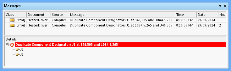
The Messages panel showing a set of DRC violations for the current PCB.
Summary
The Messages panel is a centralized listing area for the warnings, errors and status messages that are generated by operations such as compiling a project, running a design rule check, releasing a project, or using any other message-enabled features of the software.
Panel Access
To open the Messages panel, click the Messages button in the System group under the View tab: View | System | ![]() .
.
Panel Messages
The Messages panel provides a live stream of relevant message that pertain to the current operation. Where applicable, the lower section of the panel will provide further detail about the offending object(s) associated with the currently selected message.
Messages are automatically cleared (but not necessarily resolved) when a new operation that generates messages is activated.
The panel provides further details for each message class generated by the Compiler.
Message configuration
Primarily, the Messages panel is used to report the results of project compilation, listing any warnings and/or errors that the Compiler may have found whilst interrogating the design for electrical and drafting integrity. In this case, the individual messages in the panel will be directly affected by the error reporting levels and/or connection matrix defined in the Options for Project dialog.
The error reporting levels for message classes is configured in the Error Reporting tab of the Options for.. dialog, opened with the Project Options button in the Content group under the main menu Project tab. This is Project | Content | ![]() in the Schematic editor, or Project | Content |
in the Schematic editor, or Project | Content | ![]() in the PCB editor.
in the PCB editor.
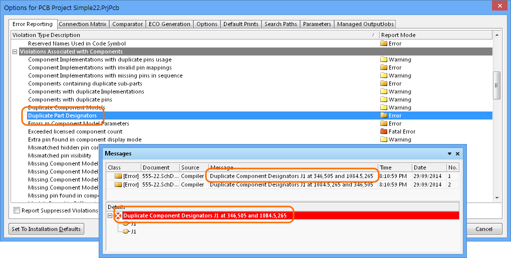
The error reporting levels defined in the Options for Project dialog will be reflected in the Message panel content.
See Project Options for more information on defining error messages in the Options for Project dialog.
Content
Along with Compiler reporting, the Messages panel will also provide warning/error/status information for other features in the software, such as PCB Design Rule Checking (DRC) and the Autorouter. The information contained within a message can be broken down into several distinct areas:
- Class – This can range from general (for example, Warning) to more specific, such as a particular design rule check category. Each degree of message will also carry a different color:
- Document – The source document where the cause of the warning/error/violation resides.
- Source – The server or engine that performed the task when the warning/error/violation was encountered (for example, the Compiler).
- Message – the actual message itself.
Each message is also date and time stamped and given a specific number within the list of messages that may appear.
Cross probing
Where applicable, a message can be cross-probed to the offending object(s) on the affected document. Cross probing takes the current view directly to the object on the associated document, or indirectly, depending on the particular source of the message. The offending object(s) will be automatically zoomed and centered (where possible) in the design editor window.
To cross probe from a message of interest, such as a Compiler error, right-click on the message and select Cross Probe from the associated context menu. Compiling the source schematic documents of a PCB project may create violation messages with the Source field entry of Compiler. Launching the cross probe command will probe directly to the offending object(s) on the relevant document in the design editor window – in the case shown below, a duplicate designator error.
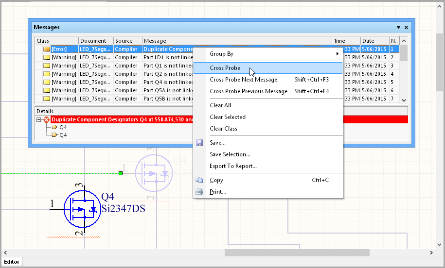
Cross-probing from a schemtic Compiler error message.
In a similar way, cross-probing from DRC error message in the panel will probe directly to the offending object on the associated document – in the below case, a PCB width rule violation.
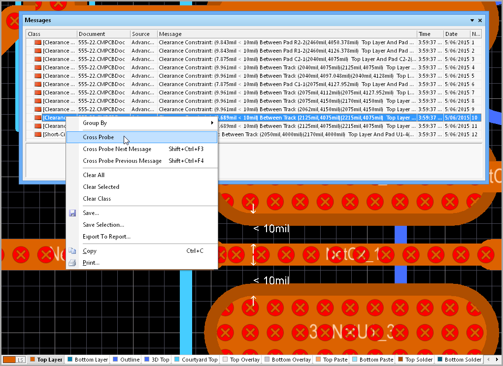
Cross-probing from a Clearance rule DRC message.
Right-click Menu
The right-click pop-up menu for the panel provides the following commands:
- Group By – Group messages together by source, class or document.
- Cross Probe – Cross probe from the selected message in the panel to the object responsible for the message in the associated document.
- Cross Probe Next Message – Cross probe to the next reported message - navigate using the Ctrl+Shift+F3 keyboard shortcut.
- Cross Probe Previous Message – Cross probe to the previous reported message - navigate using the Ctrl+Shift+F4 keyboard shortcut.
- Clear All – Clear all messages that are currently displayed in the panel.
- Clear Selected – Clear all selected messages from the panel.
- Clear Class – Clear all messages from the panel that are of the same class as the currently selected message.
- Save – Save the current list of messages in the panel as a .txt file. After launching the command, the Save Message List To File dialog appears. Use this dialog to browse to a particular destination in which to save the file and to give the file a new name (if required).
- Save Selection – Save selected messages in the panel as a .txt file. After launching the command, the Save Message List To File dialog appears. Use this dialog to browse to a particular destination in which to save the file and to give the file a new name (if required).
- Export To Report – Export selected messages in the panel as a .html file. After launching the command, a Message List.html file appears in your project.
- Copy – Copy the selected messages to the Windows clipboard.
- Print – Preview and print a report containing all messages currently listed in the panel.
Notes
- Not all messages can be cross probed. You can only cross probe from a message if it has a valid (existing) associated document, specified in the Document field of the message.
- Data may be sorted by any column by clicking on the header for that column. Clicking once will sort in ascending order. Click again to sort by descending order.
- You can change the order in which columns of data are displayed. To move a column, click on its header and drag it horizontally to the required position. A valid position is indicated by the appearance of two green positional arrows.
- Clearing messages does not necessarily mean the messages have been resolved. The same unresolved messages will be listed after performing the same command that led to the messages being generated initially. Message clearance is a visual aid when resolving errors in the design, allowing you to manually remove messages as you feel they have been resolved. The instigating command must be launched again to obtain an up-to-date picture of any violations that still exist.
- With respect to PCB/Compiler/Comparator-specific messages, if the associated document is closed, the corresponding message entries will be automatically cleared from the panel. For example, if you run a DRC Check on a PCB document, any violation messages listed in the Messages panel for that document will be cleared from the panel if the document is closed.